Components
TVS / ESD Diode Selection: The Junction-Capacitance Trap That Corrupts Your High-Speed Lines
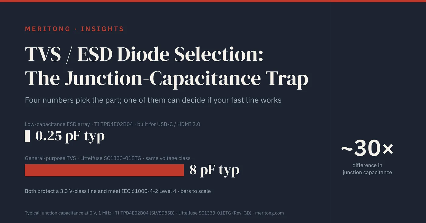
A protection diode on a USB, HDMI or CAN line can pass the ESD test and still corrupt the signal, because its junction capacitance loads the line. This guide selects a TVS diode on four parameters, capacitance among them, and shows how to check a cheaper substitute before production.
Last updated: 24 October 2026. Part values are from the named datasheets at the revisions given in the text, checked on 24 October 2026. Verify each value against the exact part and revision, and against your line's real signaling requirements, before you design one in.
The short version
A protection diode added to a USB, HDMI, Controller Area Network (CAN) or antenna line can stop that line working. The diode still does its job against an electrostatic discharge (ESD) strike, yet its junction capacitance loads the high-speed signal and corrupts it. The board then passes the ESD test and fails on signal integrity.
The remedy keeps the protection in place and changes how the part is chosen. A transient voltage suppression (TVS) diode for a fast line is selected on its capacitance as well as on its voltage. A general-purpose TVS and a purpose-built low-capacitance TVS for one 3.3 V-class line can both meet Level 4 of IEC 61000-4-2. That is the ESD standard of the International Electrotechnical Commission (IEC). Their capacitance can still differ by a factor of 30 or more. That gap can decide whether a 480 Mbps USB port works. TI recommends less than 4 pF on those lines, and a general-purpose part with 8 pF typical can make the port fail the compliance eye test or not enumerate.
A TVS is a shunt element on the line it protects, so its capacitance is added across the signal. How much added capacitance a line tolerates depends on its data rate. The slower the line, the less the capacitance counts; the faster the line, the sooner capacitance becomes the binding constraint among the four numbers below.
Each of the four numbers protects against a different failure.
| Number | What fails if it is wrong | Where it decides the part | What to verify |
|---|---|---|---|
| Stand-off voltage (VRWM) | The TVS can leak or conduct in normal operation, load the line and fail | Every line, because it sets the voltage class | VRWM at or above the line's operating voltage, with margin |
| Clamping voltage (VC) at a peak pulse current (IPP) | The protected chip sees more voltage than it survives | Lines that end in low-voltage chips, such as a USB transceiver | VC at the IPP and pulse shape of your system test, against the chip's absolute-maximum rating |
| Junction capacitance (CJ) | Signal edges slow and the high-speed link fails | USB 2.0 High-Speed and faster lines | CJ at its test condition, against the interface's capacitance budget |
| ESD and surge rating | The part fails the system-level test or is damaged by it | Every port, and for surge especially industrial inputs | IEC 61000-4-2 and IEC 61000-4-5 ratings against the system's test levels |
The four numbers that select a TVS
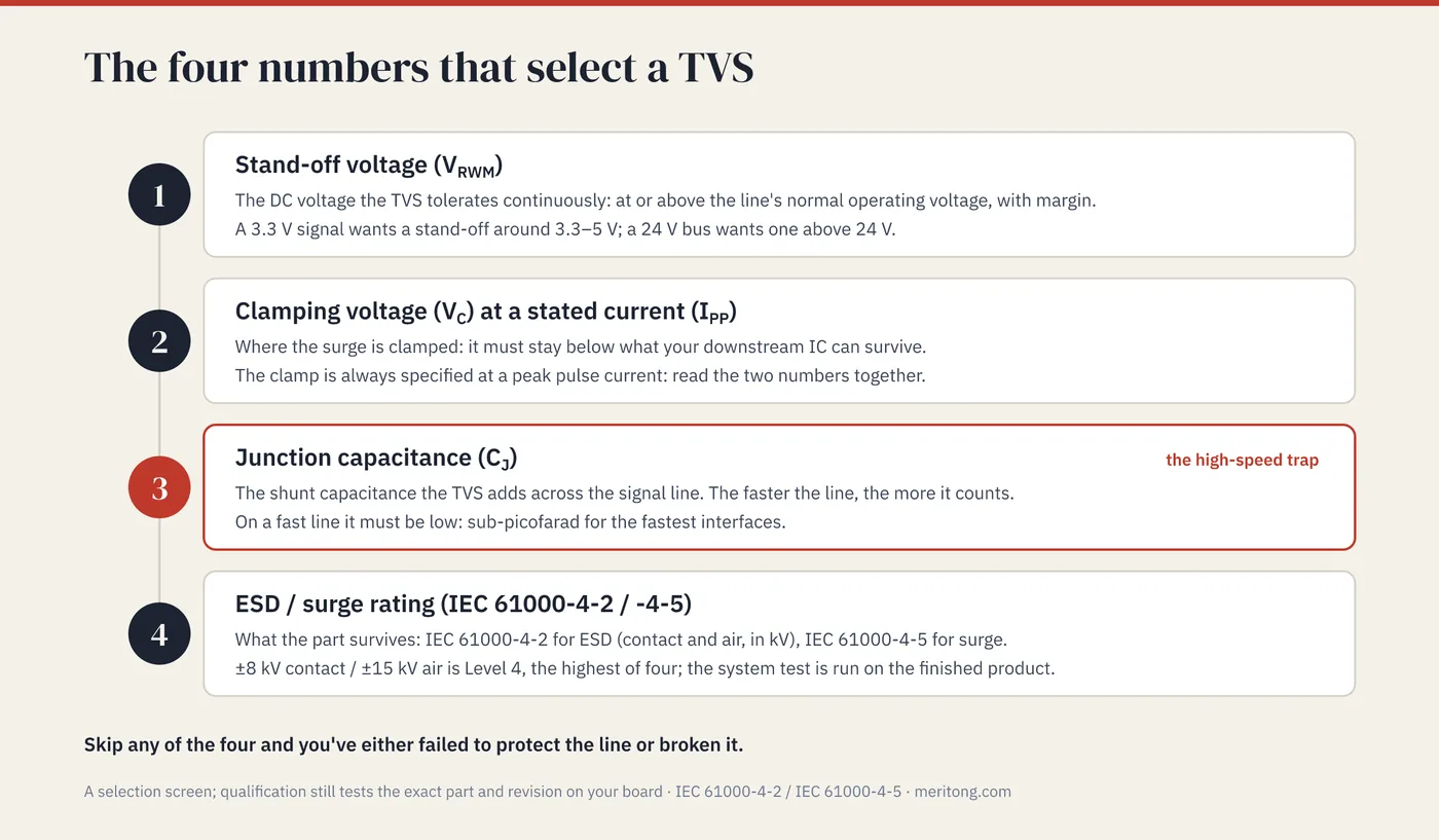
A TVS diode is selected on four parameters, and the order in which they are checked depends on the line, as the worked example shows. Skip any one of them and you have either failed to protect the line or broken it.
1. Stand-off voltage (VRWM): the DC voltage the TVS tolerates continuously without conducting, also called the reverse working voltage. It must be at or above your line's normal operating voltage, with margin. If it is chosen too low, the TVS can start to conduct during normal operation. It then leaks current and loads the line, and if the line can drive enough current, the part can overheat and fail. A 3.3 V signal wants a stand-off around 3.3–5 V, and a 24 V bus wants one above 24 V.
2. Clamping voltage (VC) at a specified peak pulse current (IPP): the voltage at which the TVS holds the line while it conducts a surge. That clamp must stay below what your downstream integrated circuit (IC) can survive. VC is always specified at a given peak pulse current. The datasheets quoted here also state the pulse shape: an 8/20 µs surge, a transmission-line pulse (TLP) or both. A clamp of a few volts at 1 A of 8/20 µs surge tells you what the protected pin sees during that strike. A TVS that clamps above what your USB physical-layer transceiver (PHY) tolerates has protected nothing, so read VC together with the IPP it is quoted at, every time.
3. Junction capacitance (CJ): the capacitance the TVS adds across the signal line. Datasheets also call it line capacitance, input/output (I/O) capacitance or diode capacitance. On a fast line it must be low, down to sub-picofarad for the fastest interfaces, and it is the parameter that corrupts high-speed lines. The next section explains how.
4. ESD and surge rating: how much abuse the part survives. IEC 61000-4-2 covers ESD, with ratings in kV for contact and air discharge. IEC 61000-4-5 covers surge, the higher-energy line transients. This rating is what an "ESD diode" exists for. A part rated to ±8 kV contact and ±15 kV air under IEC 61000-4-2 meets Level 4, the highest of the standard's four test levels. Silicon Labs' application note AN895 (Rev. 0.3, March 2021) describes IEC 61000-4-2 as a system-level test of the finished product. A part's rating is therefore one input to that test and does not replace it.
Get all four right and the protection survives the strike, clamps below the IC's limit, stays off during normal operation and leaves the signal unloaded. A design that gets 1, 2 and 4 right and never looks at 3 can pass every protection test and still break a fast line.
The trap: junction capacitance versus data rate
A TVS diode is connected across the signal line, from the line to ground, so its junction capacitance appears as a shunt capacitor on that line. On a slow line, such as a 24 V I/O pin or a push-button, a few hundred picofarads is invisible. On a fast line the same capacitance does two kinds of damage. With the line's impedance it forms a resistor-capacitor (RC) low-pass filter that rounds the signal edges, and it creates an impedance discontinuity that reflects energy back down the line. The eye in the signal's eye diagram closes, and the receiver stops seeing clean ones and zeros. USB 2.0 High-Speed runs at 480 Mbps, and USB 3.x and HDMI run faster still, so at those rates tens of picofarads are enough to corrupt the signal.
Datasheet figures show the size of the gap. The table compares parts from Texas Instruments (TI), Littelfuse, Nexperia and STMicroelectronics (ST). Each row gives the datasheet revision checked on 24 October 2026 and the section the values come from.
| Part, maker, datasheet revision and section | Built for, per the datasheet | Stand-off (VRWM) | Junction capacitance, typical / maximum (test condition) | IEC 61000-4-2 contact / air |
|---|---|---|---|---|
| TPD4E02B04, TI, SLVSD85B (July 2016), §6.3 and §6.6 | USB Type-C and HDMI 2.0; interfaces up to 10 Gbps | ±3.6 V | 0.25 pF / 0.33 pF (IO to GND, 0 V, 1 MHz, 25 °C) | ±12 kV / ±15 kV |
| SC1333-01ETG, Littelfuse, Rev. GD (07/22/22), Electrical Characteristics table | General-purpose ESD protection | 3.3 V | 8 pF / 10 pF (I/O to I/O, 0 V, 1 MHz) | ±30 kV / ±30 kV |
| PESD5Z3.3, Nexperia, v.6 (16 September 2026), Tables 5 and 6 | Titled "Low capacitance unidirectional ESD protection diodes" | 3.3 V | 172 pF / 200 pF (0 V, 1 MHz, 25 °C) | 30 kV contact |
| USBLC6-2, ST, DS4260 Rev 7 (December 2021), Table 2 and the page-1 compliance list | "USB 2.0 ports up to 480 Mb/s (high speed)" | No VRWM row; leakage tested at 5.25 V | 3.5 pF maximum (I/O to GND, VR = 1.65 V) | 8 kV / 15 kV |
| ESD2CANFD24-Q1, TI, SLVSFW5D (March 2026), §5.3 and §5.7 | CAN, CAN with flexible data-rate (CAN-FD) and related buses, at data rates up to 10 Mbps | ±24 V | 2.5 pF / 4.2 pF (0 V, 1 MHz) | ±25 kV / ±25 kV |
The table leaves out the clamping voltage because the datasheets quote it under different conditions. TI gives the TPD4E02B04's clamp for a transmission-line pulse, while ST and Littelfuse use 8/20 µs surges. The figures cannot be ranked against each other, so read each one at the IPP and pulse shape your own system test produces.
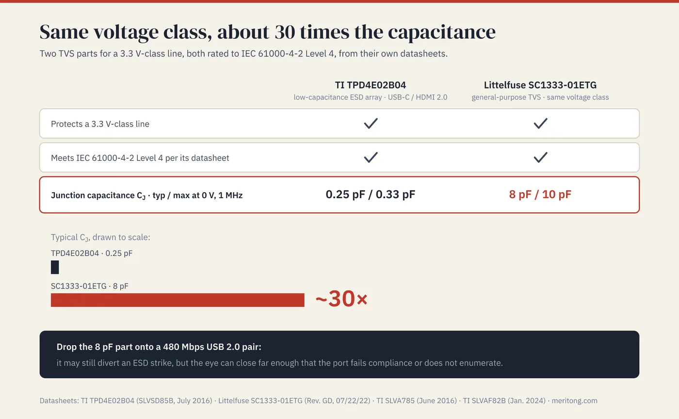
The first two rows do the same job: each part clamps a 3.3 V-class line and survives ESD at Level 4 or above. Their capacitance differs by a factor of about 30 (8 ÷ 0.25 = 32 at the typical values). TI's application note SLVAF82B, "ESD and Surge Protection for USB Interfaces" (January 2024) recommends less than 4 pF on the USB 2.0 data lines. Drop the 8 pF part onto a 480 Mbps pair and you have hung twice that ceiling across the line. The part may still divert an ESD strike, but the eye can close far enough for the port to fail the compliance eye test or not to enumerate.
Nexperia's datasheet titles its 172 pF part "low capacitance". The phrase in a title is relative, and only the picofarad figure says what the line will see.
TI's application note SLVA785, "Picking ESD Diodes for Ultra High-Speed Data Lines" (June 2016) names two criteria for selecting a TVS diode: "does this device's added capacitance still allow my signals to pass cleanly, and does this device provide the necessary protection from transient events such as ESD?"
The remedy is a low-capacitance TVS. Würth Elektronik's application note ANP143a (June 2025) calls a low-capacitance diode circuit used with the TVS "a common method to reduce the effective capacitance". Its small steering diodes connect the line to the supply rail and to ground, and they hide the larger capacitance of the clamping diode from the signal. Toshiba's 2021 technical review "Low-Capacitance TVS Diodes for High-Speed Data Communications" describes its own ESD diode arrays, which connect low-capacitance diodes in series. Toshiba says this reduces capacitance "without compromising the ESD immunity". For a line at USB 2.0 High-Speed (480 Mbps) or above, choose a low-capacitance part.
Worked example: protecting a USB 2.0 data pair
Put the four numbers together on the D+/D− pair of a USB 2.0 line running at High-Speed, 480 Mbps. High-Speed signaling swings only about 400 mV, according to TI's compliance guide SDAA519 (September 2026). The same pair also supports low- and full-speed signaling, and SLVAF82B gives 3.3 V as the typical operating voltage of the USB 2.0 data lines. The protection therefore belongs to the 3.3 V class.
The stand-off voltage (VRWM) has to cover that operating voltage, and SLVAF82B recommends at least 3.3 V. A part rated between about 3.6 V and 5.5 V covers normal operation with margin. A 24 V part is the wrong choice here, because its clamp would be far too high to protect a USB PHY.
The junction capacitance (CJ) is the number that narrows the choice on this line. At 480 Mbps you want sub-picofarad to low-single-digit picofarad capacitance per line, and SLVAF82B recommends less than 4 pF. ST's USBLC6-2 is one purpose-built part: its datasheet gives 3.5 pF maximum from I/O to ground and lists "USB 2.0 ports up to 480 Mb/s (high speed)" among its applications.
The clamping voltage (VC) has to stay low enough to protect a 3.3 V-tolerant PHY during an IEC 61000-4-2 strike. SLVA785 relates IEC 61000-4-2 test voltages to TLP current. For an 8 kV contact discharge, it says the TVS should withstand at least 16 A. Read VC for a TLP at that current and check it against your PHY's absolute-maximum rating. If the datasheet quotes VC only for 8/20 µs surges or at a lower current, ask the maker for the figure or measure it.
The ESD rating has to meet your system-level requirement under IEC 61000-4-2, for contact and for air discharge. SLVAF82B recommends at least 8 kV contact and 15 kV air for USB 2.0, which is Level 4 of the standard.
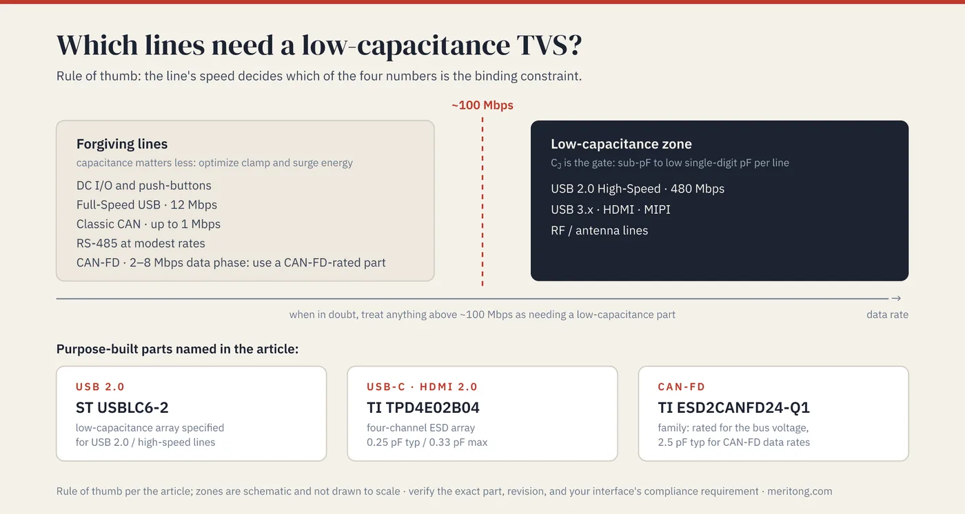
On a USB line, capacitance is a hard filter, and anything above a few picofarads is out before clamping voltages are even compared. On a 24 V industrial input, capacitance barely counts, and you would optimize clamping and surge energy instead. The line's speed decides which of the four numbers is the binding constraint.
CAN-FD falls between these two cases. TI's TCAN1044A-Q1 transceiver datasheet (SLLSFJ3D, October 2024) gives optimized CAN-FD performance at 2, 5 and 8 Mbps. Classic CAN stops at 1 Mbps, a limit that CAN in Automation (CiA) lists among those CAN-FD overcomes. The CAN-FD data phase is therefore faster than classic CAN and far slower than USB 2.0 High-Speed. TI's ESD2CANFD24-Q1 is one part built for CAN-FD lines. It has a ±24 V stand-off and 2.5 pF typical line capacitance. TI states that its family's capacitance of 3 pF typical or less supports data rates up to 10 Mbps.
What this means for a second source
A routine cost-down on a bill of materials (BOM) can go wrong at this point, whether the parts come from China or from anywhere else. Someone offers a "same 3.3 V TVS" at a better price, the stand-off voltage matches, and the part goes onto the BOM. If that line is high-speed, a matching stand-off voltage does not make the part a match. Other parts in this voltage class have 8 pF typical (the SC1333-01ETG) or 172 pF typical (the PESD5Z3.3), as the table shows. Fitted in place of a 0.25 pF array, either one still protects the line and can destroy its signal integrity. Because the board still powers up and mostly works, the failure shows as flaky enumeration, dropped packets or a unit that fails the compliance eye test. No part looks dead.
The substitution is easy to get wrong because equivalence is a property of the line as well as of the part. The capacitance that is invisible on a 24 V I/O pin is the capacitance that closes the eye on a USB pair.
A real second source for a TVS on a fast line has to meet the line's requirement on all four numbers. Its stand-off voltage has to suit the line, and its ESD and surge rating must be no lower. Its clamping voltage at the same IPP and pulse shape and its junction capacitance must be no higher. A quote or a cross-reference entry that names only the voltage class leaves the other three open. In such an entry the SC1333-01ETG at 3.3 V and the TPD4E02B04 at ±3.6 V look alike, while their CJ differs by a factor of about 30. Read the capacitance line and its test condition on any line at USB 2.0 High-Speed (480 Mbps) or faster, every time. On those lines that number can decide whether your "equivalent" TVS is equivalent or a source of field returns. A cheaper part that matches all four numbers remains a candidate second source, subject to the checks in the next section.
Verifying the choice before production
These steps screen for the principal risks. Final qualification still tests the exact part on the production board.
Obtain the current datasheet revision for the exact orderable part, and read all four numbers with their test conditions.
Compare CJ with the capacitance budget in your interface's own compliance requirement.
Read VC at the IPP and pulse shape of your system-level test, and compare it with the protected IC's absolute-maximum rating.
Follow the layout guidance in the part's datasheet and in SLVA785. Place the TVS as close to the connector as possible, avoid stubs, and keep vias on high-speed lines to a minimum.
Measure the eye diagram on the real board with and without the TVS, as the TPD4E02B04 datasheet does for USB 3.x and HDMI 2.0. Then run the system-level IEC 61000-4-2 test.
FAQ
I added an ESD diode and now my USB/HDMI line doesn't work. What happened?
One likely cause is junction capacitance that is too high for the data rate. A general-purpose TVS can present 8 pF or more, and a line at 480 Mbps or above needs sub-picofarad to low-single-digit capacitance. Rule out two other causes as well. A stand-off voltage below the line's operating voltage can make the diode leak or conduct in normal operation. Stubs or extra vias in the layout of a high-speed pair can also degrade the signal, and TI's SLVA785 treats layout as a factor in signal integrity. If capacitance is the cause, a purpose-built low-capacitance ESD array restores the line and keeps the protection in place. A USB-specific part is one example.
How do I know if my line is "high-speed" enough to care about capacitance?
As a rule of thumb, USB 2.0 High-Speed at 480 Mbps and everything faster are firmly in the low-capacitance zone. That covers USB 3.x, HDMI and MIPI, and also radio-frequency (RF) and antenna lines. Full-speed USB (12 Mbps), plain CAN, RS-485 at modest rates and DC I/O are far more forgiving. CAN with flexible data-rate (CAN-FD) falls between them, with a data phase of a few megabits per second, and TI's ESD2CANFD24-Q1 for it has 2.5 pF typical line capacitance. When in doubt, treat anything above about 100 Mbps as needing a low-capacitance part.
What capacitance number should I be under?
There is no universal figure, because it depends on the interface and its capacitance budget. The direction is clear, though. Multi-gigabit differential lines such as USB 3.x and HDMI want parts under 1 pF, and arrays like the TI TPD4E02B04 reach 0.25 pF typical. For the USB 2.0 data lines, TI's application note SLVAF82B recommends less than 4 pF. Treat anything above a few pF on a line at 480 Mbps or above with suspicion. Check your interface's own compliance requirement, and compare the datasheet CJ at its test condition against it.
What's the difference between clamping voltage and stand-off voltage?
Stand-off (VRWM) is the voltage the TVS tolerates continuously, and it is set at or above your line voltage. Clamping (VC) is the voltage the line is held to during a surge, always quoted at a peak pulse current (IPP). It must stay below your downstream IC's absolute maximum. Stand-off protects normal operation; clamping protects during the strike.
Does a low-capacitance TVS protect less?
Against ESD, a low-capacitance TVS protects to its IEC 61000-4-2 rating, like any other part. Würth Elektronik's application note ANP143a describes a common design with small steering diodes between the line and the clamping diode. The line then sees mainly their low capacitance. Toshiba describes its series-diode arrays as reducing capacitance "without compromising the ESD immunity". Surge capability is a separate figure: TI's TPD4E02B04 has 0.25 pF typical and is rated for 2 A of IEC 61000-4-5 surge (8/20 µs). Check that rating as well on any port that sees surges.
Can I reuse the same TVS across all my lines to simplify the BOM?
It is tempting, and it is risky. A part sized for your 24 V industrial input will have the wrong stand-off and probably too much capacitance for a USB line. A 0.25 pF USB part, in turn, may lack the surge energy for a heavy industrial port. Group the lines by class (high-speed data, low-speed I/O, power) and pick one part per class. That keeps the BOM short and avoids the risk of one part on every line.
My CAN bus works but the CAN-FD version doesn't, same protection. Why?
One likely reason is the TVS capacitance. CAN-FD runs its data phase much faster than classic CAN, at a few megabits per second. Capacitance that was invisible before can then slow the edges enough to matter within the shorter bit. Move to a low-capacitance TVS specified for CAN-FD and matched to the bus stand-off voltage. TI's ESD2CANFD24-Q1 is one example. Check the transceiver as well, because CAN in Automation (CiA) notes that in the data phase "the bit rate is limited by the transceiver characteristics".
Before you approve a substitute
When a TVS is offered as a substitute on a fast line, request its datasheet at the current revision and compare its CJ and test condition with the incumbent's. If its CJ is no higher than the incumbent's at a comparable test condition, repeat step 5 of the verification with the new part fitted. Measure the eye diagram on the real board first, then run the system-level ESD test.
If a cheaper TVS matches your part on stand-off voltage and leaves its capacitance an open question, I can help with component and product-architecture problems of this kind. I look at hardware, firmware and sourcing together, particularly where parts are sourced from China.
This article quotes the datasheets of the parts in the table and of TI's TCAN1044A-Q1 transceiver. It also draws on TI application notes SLVA785, SLVAF82B and SDAA519 and on Würth Elektronik's ANP143a. Further sources are Silicon Labs' AN895, Toshiba's 2021 technical review on low-capacitance TVS diodes and the CAN FD overview of CAN in Automation (CiA). IEC 61000-4-2 and IEC 61000-4-5 are referenced by their standard definitions. It is general engineering guidance. Verify the exact part and revision against your interface's compliance requirements, and confirm your protection and layout with qualified engineers.
Typical dependencies by email
Examples from real hardware audits, sent occasionally.
Working through this right now? Free intro call → or write to me →
Is this question on your desk right now?
In the free potential check you tell me the type of components you use. After 30 minutes you know whether an audit is worth it.
Free intro call