Components
Power MOSFET Second Source: RDS(on) Is the Headline; SOA and Avalanche Energy Decide Whether the Swap Survives
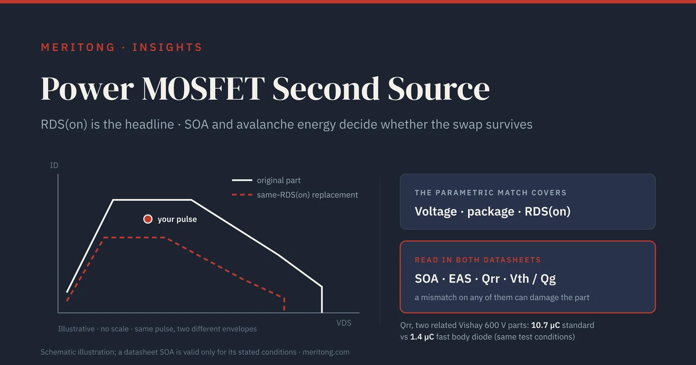
Two 600 V MOSFETs from Vishay list a maximum RDS(on) of 64 mΩ and 65 mΩ, yet a typical reverse-recovery charge of 10.7 µC and 1.4 µC under the same test conditions. Whether a power MOSFET swap survives the circuit turns on the safe operating area, the avalanche rating, the body diode and the gate, judged for one topology at a time.
Last updated: October 2026. Figures come from the datasheets and application notes named in the text, at the revisions given there, checked on 14 October 2026. Judge any substitution against the exact parts' current datasheets and your own circuit.
The short version
A power MOSFET cross-reference that starts from RDS(on), the on-resistance, starts from the headline number: it appears on the front page of the datasheet, and parametric search offers it as a sortable field. RDS(on) is a single number measured under stated conditions, so a mismatch on it is easy to see, and its consequence is conduction loss and heat.
Among the specifications that can destroy the part after a "same RDS(on)" substitution, four stand out: the safe operating area (SOA), the avalanche energy (EAS), the body diode's reverse-recovery charge (Qrr), and the gate behavior, meaning the threshold voltage (Vth) and the gate charge (Qg). Two MOSFETs with the same voltage rating and nearly the same RDS(on) can differ substantially on these. Two 600 V parts from Vishay show how far: the standard SiHG47N60E and the fast-body-diode SiHG47N60EF list a maximum RDS(on) of 64 mΩ and 65 mΩ, and a typical Qrr of 10.7 µC and 1.4 µC under the same test conditions. A mismatch on any of the four can damage the part or compromise the design, and each does so in its own way.
RDS(on) reduces to one number and sorts cleanly. The four specifications above do not: each is either a curve valid only for stated conditions or a rating whose meaning depends on your circuit, your topology or your driver. A parametric filter can shortlist on RDS(on), voltage and package; the comparison on the other four has to be made by reading both datasheets at the conditions of your circuit.
The judgment table
The table sets out, for each specification, what it governs, what a mismatch does, when it matters and what to compare on both datasheets.
| Spec | What it governs | What a mismatch does | When it matters | Compare on both datasheets |
|---|---|---|---|---|
| RDS(on) | Conduction loss | Higher loss and heat (easy to catch) | Every circuit | Maximum value at your gate voltage and junction temperature |
| SOA | Simultaneous voltage and current; linear-region use | Failure in inrush, hot-swap or linear operation | Any time spent in the linear region | SOA curves at your pulse width and case temperature, derated for your conditions |
| EAS / avalanche | Energy absorbed at an unclamped inductive turn-off | Can destroy the part when switching motors, solenoids or relays | Inductive loads without a clamp or freewheeling path | Rating method and test conditions, or avalanche current against time in avalanche at the same starting temperature |
| Qrr (body diode) | Reverse recovery in bridges and synchronous rectifiers | Shoot-through, loss, electromagnetic interference (EMI) | Bridges and synchronous rectifiers, above all at high voltage | Qrr at matching forward current, di/dt, reverse voltage and temperature |
| Vth / Qg | Compatibility with your gate driver | Incomplete turn-on, slow edges, shoot-through | Logic-level or fast gate drive | Maximum Vth at your lowest temperature (from the Vth-versus-temperature curve where given); Qg at your gate voltage; maximum gate-source voltage against your driver's highest output |
Voltage, package and RDS(on) earn a part its place on the shortlist. SOA, EAS, Qrr and gate behavior, judged for your topology, decide which part on that shortlist is fit for the circuit, and a test of the exact part in that circuit confirms it.
RDS(on) is the trap because it is the easy part
RDS(on) tells you conduction loss, and conduction loss is real. It says almost nothing, however, about whether the part survives the events in your circuit: the moment at which high voltage and high current coincide, the inductive kick when a motor or a relay is switched off, the reverse-recovery current in a bridge. Those events are governed by other specifications, so a substitution chosen on RDS(on) alone has been chosen on the one axis you already had covered. The judgment has to be made on the axes you have not yet examined.
SOA: same package, different envelope
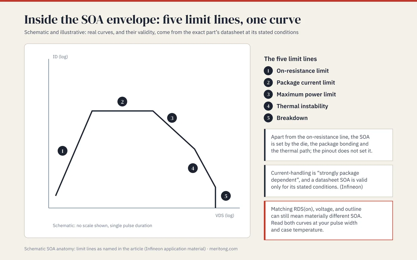
The safe operating area is the envelope of voltage and current that the MOSFET can withstand simultaneously, for a given time, before it fails. Infineon's application note AP99007, "Linear Mode Operation and Safe Operating Diagram of Power-MOSFETs" (V1.1, May 2017) names five limit lines that bound it: the RDS(on) limit, the current limit, the maximum-power limit, the thermal-instability limit and the breakdown-voltage limit. For a second source, what matters is where those lines originate. The current limit is, in Infineon's words, "strongly package dependent", and the power and thermal-instability limits follow from the die and its thermal path; the pinout and the RDS(on) do not determine them. The same note states that "the SOA diagram in datasheets is only valid for the given conditions" and that other application conditions require a derating.
It follows that two parts which match on RDS(on), voltage and outline can have materially different SOA. Where your MOSFET spends time in the linear region, as it does in inrush limiting, hot-swap, a slowly charging load or a linear pass element, SOA decides whether it survives, and a matching RDS(on) does not establish that part of the envelope. Read both SOA curves at your pulse width and case temperature, and derate both for your conditions in the same way.
Avalanche (EAS): energy from an inductive turn-off
When current through an inductance, whether a motor winding, a solenoid or a transformer, is switched off and no clamp or freewheeling path takes it, the inductor drives the drain voltage up until the MOSFET avalanches, and at least the stored energy is dissipated in the device. A MOSFET rated for this can absorb a defined single-pulse avalanche energy (EAS); a part without such a rating, or with less capability than your event demands, can fail. EAS is a separate datasheet entry. Infineon's IRL80HS120 datasheet (V2.2, 2019-12-13) lists in its Table 4 an EAS of 22 mJ, under the test conditions in its footnote (starting junction temperature (TJ) 25 °C, inductance L = 0.8 mH, gate resistance RG = 50 Ω, avalanche current IAS = 7.5 A); its Table 5 gives a maximum RDS(on) of 32 mΩ at a gate-source voltage of 10 V.
The difficulty for a second source is that the avalanche number does not compare across parts on its own. Vishay's application note AN-1005, "Power MOSFET Avalanche Design Guidelines" (Rev. 06-Dec-11) describes three rating practices: a thermal-limit rating, a statistical rating from devices tested to failure (on some parts marked "EAS (tested)", usually alongside a thermal-limit rating), and no avalanche rating at all. It warns that "it is not sufficient to merely compare the numeric values of avalanche energy which appear in datasheet tables." onsemi's application note AND90158/D (Rev. 1, May 2023) plots the peak avalanche current (Ipk) against the time in avalanche (tav) and gives the method: "compare the Ipk vs tav plot data at the same Tj(initial) temperature and not compare single UIS rating values"; onsemi's note uses UIS for unclamped inductive switch-off.
RDS(on) and avalanche capability are separate ratings, and a match on one does not establish the other. A replacement can match your RDS(on) and have a lower avalanche rating, a rating made by a different method, or none at all, and a comparison of RDS(on) will show none of the three. In a design that switches inductive loads without a clamp, compare the avalanche ratings by method and test conditions.
Qrr: the body diode in bridges and synchronous rectifiers
Every power MOSFET has an intrinsic body diode, and in bridge and synchronous-rectifier topologies that diode conducts and then has to turn off. Its reverse-recovery charge (Qrr) is the charge swept out during that turn-off. A large Qrr means a large reverse-recovery current spike, which in a half-bridge appears as shoot-through, extra loss and EMI. Vishay's application note AN847 (Rev. 15-Dec-14) analyses a zero-voltage-switching (ZVS) full bridge in which a body diode has not recovered before its own switch turns off, and adds that the switches "may not fail immediately" but keep dissipating heat until they fail. The effect grows with voltage class: AN847 puts the Qrr of a 100 V MOSFET in the tens of nC and that of a standard 600 V superjunction device at several µC. For its OptiMOS parts in synchronous rectification, Infineon's note cited below treats Qrr, to a first approximation, as a minor loss term.
Qrr can differ several-fold between closely related parts. AN847 compares Vishay's standard SiHG47N60E-GE3 with the fast-body-diode SiHG47N60EF-GE3 and gives 11 µC against 1.1 µC; it states that fast-body-diode MOSFETs are typically "designed to have a 5 x to 10 x reduction" in Qrr. The current datasheets of the two parts (SiHG47N60E, Rev. N, 24-Jul-17; SiHG47N60EF, Rev. H, 27-Feb-17) list in their specifications tables a maximum RDS(on) of 64 mΩ and 65 mΩ at a gate voltage of 10 V and, under the same test conditions (TJ 25 °C, forward current 24 A, di/dt 100 A/µs, reverse voltage 400 V), a typical Qrr of 10.7 µC and 1.4 µC. AN847's 11 µC matches the standard part's datasheet row at a reverse voltage of 25 V; its 1.1 µC and the datasheet's 1.4 µC for the fast-body-diode part are different figures, so compare the datasheet rows of both candidates at matching conditions.
Datasheet Qrr is itself a measurement under fixed conditions. Infineon's application note "OptiMOS™ device selection for synchronous rectification" (V1.1, 2023-02-15) explains that the Qrr quoted in datasheets is measured to the standards of JEDEC, the semiconductor industry's standards body, and includes part of the MOSFET's output charge, and that in a real circuit the effective value depends on how long the body diode conducts before turn-off. Swap a fast-body-diode part for a standard one in a bridge and you can turn a clean design into a hot, noisy and marginal one.
Vth and Qg: the gate the driver has to drive
The gate remains, and here the question is compatibility with a component the substitution leaves in place: your driver. Two specifications decide whether the existing gate driver switches the replacement cleanly, the threshold voltage (Vth) and the gate charge (Qg). A part with a higher Vth may not fully enhance from a logic-level drive that was adequate for the original. Nexperia's application note AN90001, "Designing in MOSFETs for safe and reliable gate-drive operation" (Rev. 1.1, 29 October 2024) states, in its worst-case analysis of its own devices, that the threshold of a standard-level device "can be as high as 4.5 V" at the lower temperature limit, so that with a 5 V driver output such a device "may not be suitable". The same note explains that the threshold falls as the junction warms, which matters for holding the part off at high temperature. The gate limit cuts the other way as well: AN90001 gives a maximum gate-source voltage (VGS(max)) of typically 10 V for Nexperia's logic-level and 20 V for its standard-level automotive devices at the maximum rated temperature, and warns that other datasheets often state VGS(max) at 25 °C, which "will make that MOSFET appear more capable on first review." The same note adds that Nexperia's own more recent datasheets also state the maximum at 25 °C, to align with other vendors. A logic-level replacement for a standard-level part, driven at the gate voltage the original was designed for, may exceed its own VGS(max).
A part with much higher Qg switches more slowly or overloads the driver, which raises switching loss and, in a bridge, risks shoot-through from sluggish edges. Vishay's application note AN608A (Rev. 16-Feb-16) works through how a part's gate-charge parameters set its switching times. To your driver, a "same RDS(on)" MOSFET with a different gate profile is a different part.
Judge by topology
The specifications that matter differ from circuit to circuit, which is why a single parametric sort cannot settle them. Let the topology tell you which of them to check hardest.
Simple switch / load switch, well within ratings: RDS(on) and thermal behavior dominate, though SOA is still worth a glance for inrush.
Inrush limiter, hot-swap or anything in the linear region: SOA is the make-or-break specification, since the part spends real time at high voltage and high current together.
Switching a motor, solenoid, relay or other inductive load without a clamp: the avalanche rating decides, since the turn-off energy has to go into the MOSFET. With a clamp or freewheeling diode in place, that path takes the energy instead, and its own rating belongs in the check.
Half-bridge, full-bridge or synchronous rectifier: Qrr (above all at high voltage) and gate timing decide, since body-diode recovery and shoot-through determine whether the stage runs cool or overheats.
Logic-level or fast-switching gate drive: check Vth and Qg against your specific driver.
A replacement that is ideal for a load switch can be a poor choice for a bridge at the identical RDS(on), because the bridge depends on a specification the load switch never exercised. Naming your topology first changes the task from finding a same-RDS(on) part to finding a part that survives this circuit.
These checks identify the principal risks of a substitution and screen candidates; qualification must still test the exact part, by its full orderable part number, in the intended circuit at its worst-case corners.

Why a parametric filter cannot make this judgment
Parametric search sorts on fields that hold a single value, such as voltage, RDS(on), current and package. The four specifications above resist that treatment: SOA is a curve valid only for stated conditions; an avalanche rating means something only alongside its method and test conditions; the effect of Qrr depends on your topology and on how it was measured; gate behavior depends on your driver. Some distributor filters do list a maximum Vth and a Qg, but each at one stated current or gate voltage; the threshold at your lowest temperature, the charge at your drive voltage, an SOA curve and the method behind an avalanche rating still have to be read in both datasheets. A filter therefore shortlists on the easy axes and leaves the rest to that reading. That reading is the work a power-MOSFET second source requires; the filter produces the shortlist.
Before you commit: a verification sequence
Collect the documents: both current datasheets, with revision and date, and for the avalanche rating the manufacturer's statement of how it was rated.
SOA: overlay both curves at your longest pulse and highest case temperature, apply the derating your conditions require, and check every operating point, including start-up and fault cases.
Avalanche: if the circuit can avalanche, work out the energy and current your inductance delivers, then compare both parts' ratings at the same conditions, or their Ipk against tav curves at the same starting temperature. Treat a part without an avalanche rating as unrated for that duty.
Body diode: compare Qrr at matching forward current, di/dt, reverse voltage and temperature, then check dead time and switching-node ringing on the board.
Gate: compare the maximum Vth at your lowest operating temperature (from the Vth-versus-temperature curve where given, or from the manufacturer) with the driver's output high level, Qg at your gate voltage with the driver's current capability, the off-state margin at your highest temperature, and the replacement's VGS(max) against your driver's highest output, noting the temperature at which each datasheet states it.
Test the exact part: build with the full orderable part number and exercise inrush, inductive turn-off and bridge switching at the temperature corners before committing to production.
FAQ
If two MOSFETs have the same RDS(on), aren't they interchangeable?
They are not. RDS(on) sets conduction loss and one edge of the SOA. A match on it does not establish a match on the rest of the SOA, avalanche energy, body-diode recovery or gate behavior, any of which can differ greatly between parts with nearly identical RDS(on) and, in the right circuit, destroy the part or the design.
What's SOA and why can't a parametric tool compare it?
The safe operating area is the voltage, current and time envelope the device withstands, bounded by limits that the die, the package and the thermal path set. Because it takes the form of a curve, valid only for stated conditions, it does not reduce to a filterable field. Read both parts' SOA curves at your operating point.
When does avalanche energy (EAS) matter?
It matters whenever current through an inductance (a motor, solenoid, relay or transformer) is switched off without a clamp or freewheeling path. The inductor drives the MOSFET into avalanche, and EAS states how much of that energy the device can absorb under the datasheet's test conditions. Manufacturers rate avalanche by different methods, so compare the method and the conditions as well as the number; a replacement with the "same" RDS(on) can still fail.
Does the body diode really matter for a swap?
In bridges and synchronous rectifiers it does, above all at high voltage, because the body diode's reverse-recovery charge (Qrr) drives shoot-through and loss. Vishay's application note AN847 states that fast-body-diode MOSFETs are typically designed for a five to ten times lower Qrr than standard parts, so a swap between the two types changes the circuit's behavior even within one product family.
What's the safest way to cross-reference a power MOSFET?
Shortlist on voltage, package and RDS(on). Then, for your topology, compare SOA at your pulse width and temperature, the avalanche rating by method and conditions against your inductive-switching energy, Qrr at matching conditions where the circuit is a bridge, and Vth and Qg against your gate driver. These steps screen candidates; the exact part still has to be tested in your circuit.
Close
A MOSFET cross-reference on RDS(on) produces a shortlist. The decision is made in the SOA curve, the avalanche rating, the body diode and the gate, and it is made for one topology at a time. A second source buys supply security and leverage in price negotiations; it costs a qualification cycle, whose depth depends on the circuit. For a load switch well within its ratings, matching voltage, package, RDS(on) and thermal behavior may be most of the work. For a hot-swap stage, an unclamped inductive load or a bridge, the substitution is safe only once those curves and ratings have been compared and the exact part has been tested.
If you are qualifying a second source for a power stage and want the SOA, avalanche and gate questions read against the rest of the design, I help with hardware-component and product-architecture problems of this kind, particularly where China sourcing is involved, and I look at the hardware, firmware and sourcing together.
This article illustrates real MOSFET specifications with figures from the datasheets and application notes of the parts named. It is general engineering guidance. It does not specify the behavior of any particular device. Judge any substitution against the exact parts' current datasheets and validate it in your circuit.
Typical dependencies by email
Examples from real hardware audits, sent occasionally.
Working through this right now? Free intro call → or write to me →
Is this question on your desk right now?
In the free potential check you tell me the type of components you use. After 30 minutes you know whether an audit is worth it.
Free intro call