Components
The Op-Amp Cross-Reference Checklist: Five Specs to Check Before a "Jellybean" Swap
Two dual op-amps can share an 8-pin package and the same pin assignment and still differ by orders of magnitude on the specifications a circuit depends on. Supply range and quiescent current can disqualify a part outright; five further specifications then decide whether the swap holds up, and this checklist works through all five before you approve an op-amp second source.
Last updated: October 2026. Figures come from the manufacturers' datasheets at the revisions listed in the table below, checked on 21 October 2026. Verify them against the exact part and revision before you design one in.
The short version
Two dual op-amps can share an 8-pin package and pin assignment and still differ by orders of magnitude on the specifications a circuit depends on. The LM358, TL072, NE5532, MCP6002 and OPA2340 are all sold as duals in 8-pin packages with the same pin assignment. They are not interchangeable. A swap made on price or availability alone can cost you DC accuracy. It can also clip the output short of a rail, slew-limit the signal or raise the noise floor. The circuit can still work on the bench in a loose sense and then fail its real specification in the field.
Supply range and quiescent current come first, because a mismatch there can disqualify the part outright. Five specifications then identify the principal risks of the swap. Read all of them on both datasheets before you approve an op-amp second source. A test of the exact part in your own circuit completes the qualification.
A shared package and pin assignment establish that two parts are mechanically interchangeable, and they establish nothing beyond that. Offset, bias current, bandwidth, output swing and noise decide whether the circuit still meets its requirement. These can differ widely between parts that share a footprint. Across the six parts in the table, typical offset spans about three orders of magnitude (2 µV to 3 mV). Typical input bias current spans six (0.2 pA to 200 nA). Which of them decides in a given design depends on what that design relies on.
The six datasheets behind the figures
The table lists the figures this article quotes from the Texas Instruments (TI) and Microchip datasheets. They apply at 25 °C and under each datasheet's stated test conditions. The input stages are bipolar, FET (field-effect transistor) or CMOS (complementary metal-oxide-semiconductor). Offset, bias-current and swing values are marked typ (typical) or max (limit). Bandwidth and slew-rate values are typical, and supply ranges are the datasheets' recommended or specified ranges.
| Part (datasheet, revision) | Input stage | Offset voltage | Input bias current | Gain-bandwidth · slew rate | Output swing below V+ | Supply range |
|---|---|---|---|---|---|---|
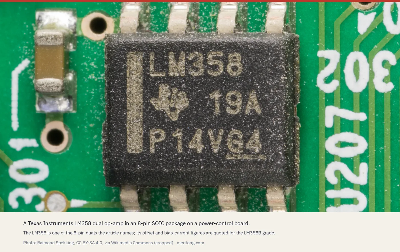
| TI LM358B (SLOS068AB, Oct 2024) | Bipolar | ±0.3 mV typ, ±3.0 mV max | 10 nA typ, 35 nA max | 1.2 MHz · 0.5 V/µs | 1.35 V typ at 50 µA, 1.61 V max at 5 mA | 3 V to 36 V |
| TI TL072, C grade (SLOS080W, Jul 2025) | FET | 3 mV typ, 10 mV max | 65 pA typ, 200 pA max | 5.25 MHz · 20 V/µs | 1.5 V typ, 3 V max (±15 V, 10 kΩ) | 4.5 V to 40 V |
| TI NE5532 (SLOS075K, Dec 2025) | Bipolar | 0.5 mV typ, 4 mV max | 200 nA typ, 800 nA max | 12 MHz unity-gain · 5 V/µs | Not specified in this revision | ±5 V to ±15 V |
| Microchip MCP6002 (DS20001733L, Mar 2020) | CMOS | ±4.5 mV max | 1 pA typ | 1.0 MHz · 0.6 V/µs | 25 mV max (5.5 V, 10 kΩ) | 1.8 V to 6.0 V |
| TI OPA2333 (SBOS351E, Dec 2015) | CMOS, zero-drift | 2 µV typ, 10 µV max | 70 pA typ, 200 pA max | 350 kHz · 0.16 V/µs | 30 mV typ, 50 mV max (10 kΩ) | 1.8 V to 5.5 V |
| TI OPA2340 (SBOS073C, Aug 2016) | CMOS | ±150 µV typ, ±500 µV max | 0.2 pA typ, 10 pA max | 5.5 MHz · 6 V/µs | 10 mV typ (10 kΩ) | 2.7 V to 5 V |
The five TI datasheets were the current revisions on 21 October 2026, and TI listed all five parts as active.
Spec 1. Input offset voltage (and drift): your DC accuracy
Input offset voltage (VOS) is a small DC error voltage that acts as if it were in series with the op-amp's input. It adds directly to your signal and is amplified by your gain. For that reason it is often the specification that matters most in a circuit that measures a real quantity. A sensor front-end, a current-sense amplifier and a precision reference buffer are such circuits.
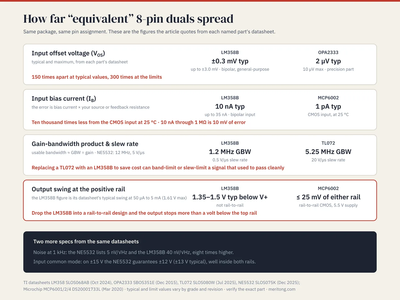
A general-purpose "jellybean" LM358B specifies an input offset of ±0.3 mV typical and ±3.0 mV maximum. A precision part such as the OPA2333 specifies its offset in microvolts: 2 µV typical, 10 µV maximum. The OPA2333 is therefore 150 times tighter at typical values and 300 times at the limits. Suppose you replace the precision amplifier with the general-purpose part to save cost. A design that relied on sub-millivolt accuracy can then have up to 3 mV of error at 25 °C, and up to 4 mV over −40 to +85 °C. In a high-gain stage that error can dominate your signal.
The companion specification is offset drift, in µV/°C, which describes how far the offset moves with temperature. A room-temperature calibration cannot remove that part of the error, so a design calibrated once and then operated across its temperature range needs a low-drift part. General-purpose parts drift far more than precision amplifiers. The LM358B lists ±3.5 µV/°C typical and 11 µV/°C maximum, against 0.02 µV/°C typical and 0.05 µV/°C maximum for the OPA2333. If your circuit amplifies a small DC or low-frequency signal, match offset and drift first.
Spec 2. Input bias current (and input type): the error at high source impedance
Input bias current (IB) is the small current the op-amp's inputs draw. Flowing through the source or feedback resistance, it becomes a voltage error. With a low-impedance source that error is negligible. Photodiodes and piezo sensors are high-impedance sources, as are high-value dividers and pH probes. With them the error can swamp the measurement, and the difference between bipolar and CMOS inputs decides the outcome.
A bipolar-input part like the LM358B draws bias current in the tens of nanoamps: 10 nA typical, 35 nA maximum. A CMOS-input part like the MCP6002 draws about 1 pA typical at 25 °C, roughly ten thousand times less. That figure rises with temperature, to 19 pA typical at 85 °C and 1,100 pA at 125 °C. Put 10 nA through a 1 MΩ source and you have 10 mV of error before your signal even starts. The picoamp CMOS part makes 1 µV, a ten-thousandth of that. So "replace the op-amp with a cheaper equivalent" can mean swapping a CMOS input for a bipolar one. That swap can swamp a high-impedance measurement, even though both parts are dual op-amps in the same package. Match the input type to your source impedance. A high-impedance source wants a CMOS or junction field-effect transistor (JFET) input with its low bias current, and a low-impedance source can tolerate a bipolar one.
Spec 3. Gain-bandwidth product and slew rate: your speed ceiling
Two specifications bound how fast an op-amp can go. Gain-bandwidth product (GBW) sets the usable bandwidth at your closed-loop gain (bandwidth ≈ GBW ÷ gain). Slew rate, in V/µs, sets how fast the output can move for large signals. With too little of it, a fast or large-amplitude waveform comes out as a distorted triangle.
The LM358B lists 1.2 MHz GBW and a slew rate of 0.5 V/µs, adequate for DC and audio-band sensor work and too slow for anything fast. The older LM358 grade in the same datasheet lists 0.7 MHz and 0.3 V/µs. The TL072 is much quicker at 5.25 MHz GBW and 20 V/µs, although its NS and PS packages and its M grade are specified at 3 MHz. The NE5532's two figures do not move together. Its table lists a 12 MHz unity-gain bandwidth, wider than the TL072's, but its slew rate of 5 V/µs is a quarter of the TL072's. The revision history records both as changed from 10 MHz and 9 V/µs. The feature description in the same revision still says 10 MHz, and its slew-rate paragraph prints "9V/ms". Confirm both figures with TI if your design depends on them.
Replacing an LM358B with a TL072 raises both figures, although the other checks still apply: the TL072's input range stops short of the negative rail. Replacing a TL072 with an LM358B to save cost can slew-limit or band-limit a signal that used to pass cleanly. If your circuit handles more than low audio frequencies or any fast edge, check the replacement's GBW at your gain and its slew rate. Both should clear your signal with margin.
Spec 4. Input and output range (rail-to-rail or not): the highest-value check for single-supply, low-voltage designs
The LM358B, the TL072 and the NE5532 are not rail-to-rail parts, and none of their datasheets claims rail-to-rail operation. Their outputs cannot swing all the way to the supply rails, and their input common-mode ranges stop short of one or both rails. The resulting failure does not show up until the signal reaches a rail.
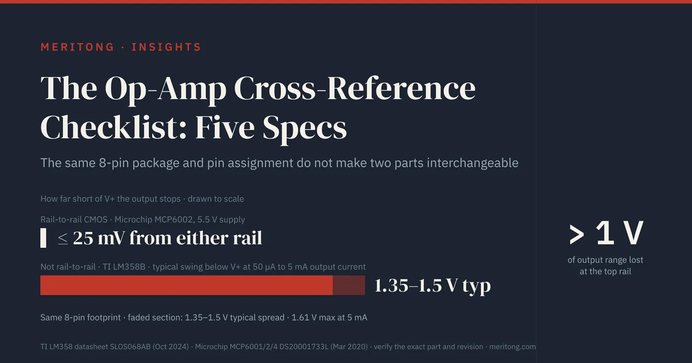
With a 10 kΩ load to V− at 5 V, the LM358B output typically comes within 5 mV of the negative rail. When it sinks 1 mA it typically stays 0.75 V above that rail (1 V maximum), and it cannot reach the positive rail at all. Its datasheet gives the swing below V+ as 1.35 V typical at 50 µA and 1.5 V typical at 5 mA, with a 1.61 V maximum. Its input common-mode range runs from V− up to 1.5 V below V+ (2 V over temperature). The NE5532 on ±15 V guarantees ±12 V of common-mode range (±13 V typical), well inside both rails.
Now take a modern single-supply design built around a rail-to-rail CMOS part. The MCP6002 swings to within 25 mV of either rail at a 5.5 V supply, and the OPA2340 to within 10 mV with a 10 kΩ load. The design assumes that output range. Drop an LM358B into that socket and the output stops more than a volt below the top rail. Your usable range collapses, and a digital-to-analog converter (DAC) buffer can no longer reach full scale. A comparator with its threshold near V+ fails as well, mainly because the LM358B's input common-mode range ends 1.5 V below V+. The NE5532 fails earlier, at the supply gate, because its recommended operating conditions start at ±5 V. The reverse swap is safer only at the same low supply, and there it wastes the rail-to-rail part's advantage. In a socket that runs the LM358B above 7.0 V, an MCP6002 would exceed its absolute maximum rating, which the supply check catches first.
The clipping appears only when the signal approaches the rail the replacement cannot reach. A bench test that never drives the signal to that rail can therefore pass a design that fails at the extremes it was built to cover. This is why the failure is silent.
For single-supply, low-voltage designs this is the highest-value line on the checklist. Compare the replacement's output swing and input common-mode range with what your circuit needs at your supply voltage. Where the datasheet specifies them, both figures are in its electrical-characteristics table, under headings such as "voltage output swing from rail" and "common-mode voltage range".
Spec 5. Noise and stability (capacitive-load tolerance)
The fifth check covers two related properties. Voltage-noise density, in nV/√Hz, decides whether a low-level signal survives. The NE5532 is a low-noise part at 5 nV/√Hz at 1 kHz, while the LM358B lists 40 nV/√Hz at the same frequency, eight times higher. Replace the low-noise amplifier with a general-purpose one in a microphone preamp or a sensor front-end, and you can raise the noise floor audibly or measurably.
Stability with capacitive loads is the other half, and op-amps differ in how much capacitance they can drive before ringing or oscillating. The LM358B datasheet gives a capacitive load drive of 100 pF, while the MCP6002 datasheet states a typical 45° phase margin with a 500 pF load. The two figures are specified differently, so compare like with like on both datasheets. A part that drove your cable or analog-to-digital converter (ADC) input stably can be replaced by one that does not. If you drive a capacitive load, check the replacement's capacitive-load tolerance and its unity-gain stability. Long lines, filter capacitors and ADC sample capacitors are all capacitive loads.
Don't forget: supply voltage and quiescent current
Two gating specifications come before the five. A mismatch on either can disqualify a part before you compare performance at all.
Supply-voltage range: the NE5532 is specified for ±5 V to ±15 V. The MCP6002 runs from a single 1.8 V to 6.0 V supply and the OPA2333 from 1.8 V to 5.5 V. The MCP6002's absolute maximum is 7.0 V, so ±15 V would exceed that rating. The reverse fails as well: a part specified for ±5 V to ±15 V cannot be used within its recommended operating conditions in a 3.3 V single-supply design.
Quiescent current: for battery or always-on designs, count the supply current per amplifier. The faster parts here draw more: the NE5532 lists 6 mA typical for both amplifiers and the OPA2340 750 µA per amplifier, against 100 µA for the MCP6002. Precision does not imply high current, since the OPA2333 lists 17 µA. Confirm first that the replacement runs on your actual supply and fits your power budget. Then work through the five performance checks.
The checklist, in order
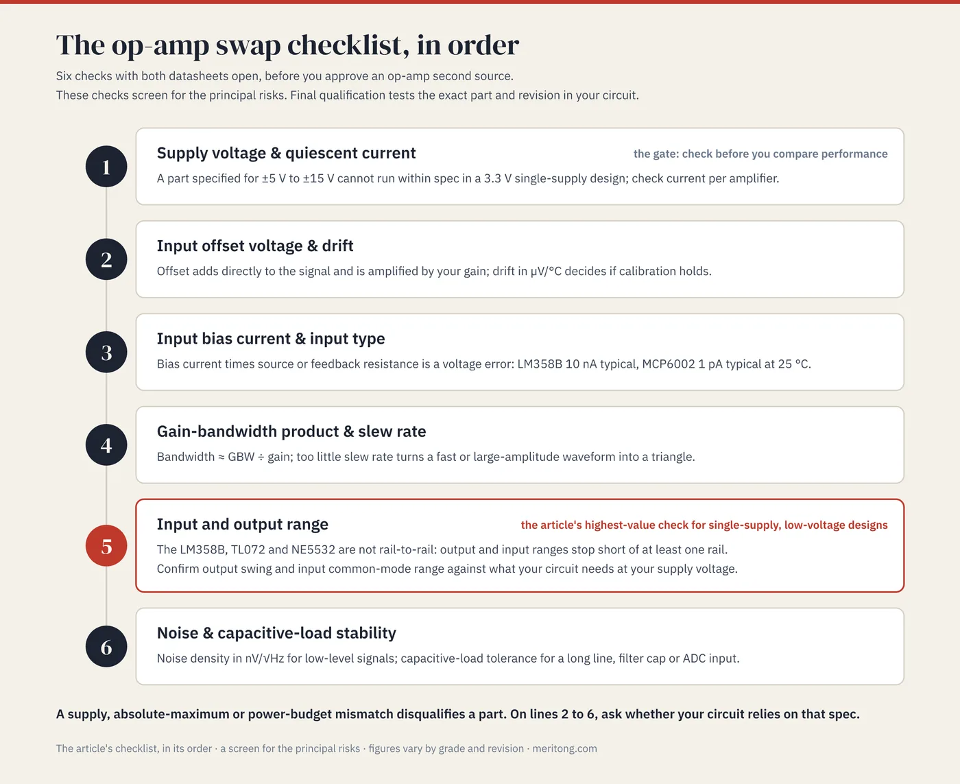
Run these six checks with both datasheets open before you approve an op-amp second source:
Supply & quiescent current: does it run on my rails and fit my power budget?
Offset voltage & drift: is my DC accuracy preserved?
Input bias current & type: does it match my source impedance (CMOS or JFET for a high-impedance source)?
GBW & slew rate: does it clear my bandwidth and signal speed at my gain?
Input/output range: is it rail-to-rail where my circuit needs it?
Noise & capacitive-load stability: are my noise floor and load drive preserved?
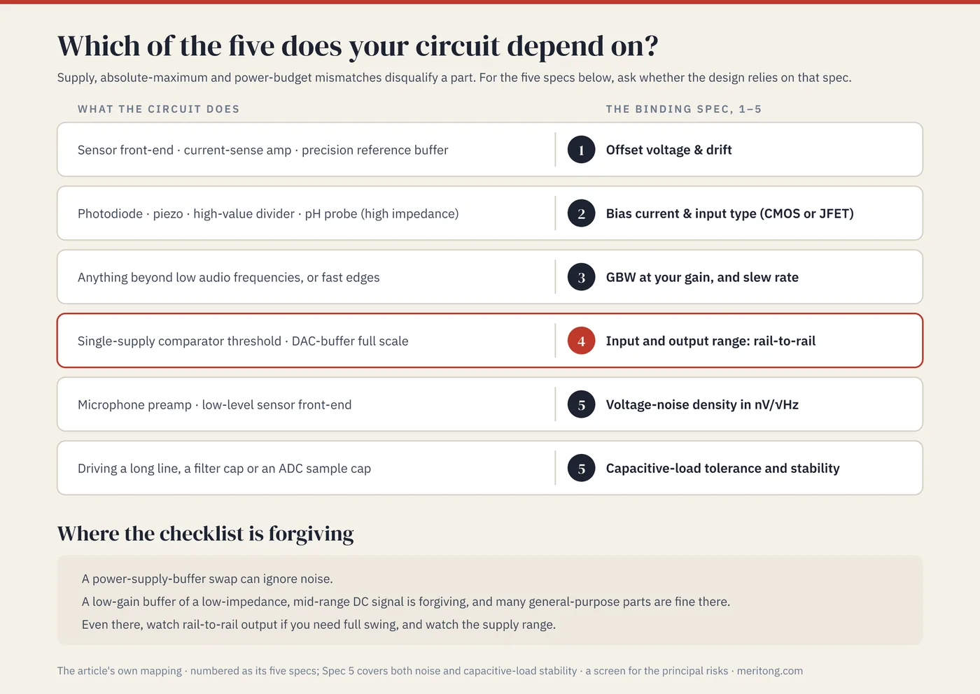
A mismatch on line 1 disqualifies the part when the replacement cannot run on your supply, would exceed an absolute maximum rating or would break your power budget. On lines 2 to 6 a mismatch counts only where your circuit relies on that specification. A power-supply-buffer swap can ignore noise. A photodiode amplifier depends on bias current, and a single-supply comparator on rail-to-rail output. The checklist helps you find which of the five your design depends on.
FAQ
Aren't all dual op-amps basically interchangeable?
Parts with the same package and pin assignment are interchangeable only mechanically. Their electrical specifications can still differ widely. Across the six parts in the table, typical offset spans about three orders of magnitude (2 µV to 3 mV). Typical input bias current spans six (0.2 pA to 200 nA). A swap is safe only after you confirm that the specifications your circuit relies on are preserved. The checklist above is for that confirmation.
What happens when a non-rail-to-rail part replaces a rail-to-rail one?
Take a single-supply design built around a rail-to-rail part such as the MCP6002, and fit an LM358B. The output then stops more than a volt below the positive rail, and your usable range or full scale is lost. The TL072 and the NE5532 are not rail-to-rail either, and the NE5532's supply range rules it out at low voltage before the swing does. Check output swing and input common-mode range at your supply voltage.
When does input bias current matter?
It matters when your source impedance is high: photodiodes, piezo sensors, high-value dividers and electrochemical probes. Bias current multiplied by source impedance is a voltage error, so compute IB × R for your source. A bipolar part can add millivolts or more, with 10 nA typical for the LM358B and 200 nA for the NE5532. A CMOS part at 1 pA adds 1 µV across 1 MΩ but 1 mV across 1 GΩ. The OPA2333's 70 pA typical becomes 70 mV across 1 GΩ, so picoamps matter at gigaohm sources too. High-impedance sources want CMOS or JFET inputs, and even then the product IB × R decides.
Can I always upgrade to a "better" op-amp?
You cannot do so blindly. A faster or precision part can draw more current or need a different supply, and it can tolerate capacitive loads less well or be worse for a specific noise profile. Precision can cost speed as well: the OPA2333 lists 350 kHz GBW against the LM358B's 1.2 MHz. "Better on paper" can still break your power budget or your stability. Run the same checklist, including supply and quiescent current, even when trading up.
Why is my circuit noisier after the op-amp swap?
One likely cause is a low-noise part replaced by a general-purpose one with a much higher noise density. The NE5532 lists 5 nV/√Hz at 1 kHz, and the LM358B lists 40 nV/√Hz. In audio or low-level sensor front-ends that raises the noise floor audibly or measurably. Oscillation on a capacitive load can also show up as added noise, so check stability as well (Spec 5). Match the voltage-noise density for any low-signal stage.
Do these differences matter for a simple buffer or DC gain stage?
They matter less. A low-gain buffer of a low-impedance, mid-range DC signal is forgiving, and many general-purpose parts are fine there. Even there, watch the rail-to-rail output if you need full swing, and watch the supply range. The more your circuit demands from one specification, the more closely that specification must match.
Which spec decides, and what to measure
Which specification decides depends on the circuit: offset for a sensor front-end, bias current for a photodiode, output range for a single-supply DAC buffer. Where a datasheet leaves a figure out, as the current NE5532 revision does for output swing, a measurement on the exact part in your circuit has to supply it.
If an op-amp swap looks safe on the footprint and you want it checked against what your circuit relies on, I help with hardware-component and product-architecture problems of this kind. I work particularly where China sourcing is involved, and I look at hardware, firmware and sourcing together.
Figures come from the six datasheets listed in the table above, at the revisions given there, checked on 21 October 2026. They are typical or limit values under each datasheet's stated conditions and vary by grade and revision. This is general engineering guidance. Verify the exact part and revision against your circuit's requirements, and have the design confirmed by qualified engineers.
Typical dependencies by email
Examples from real hardware audits, sent occasionally.
Working through this right now? Free intro call → or write to me →
Is this question on your desk right now?
In the free potential check you tell me the type of components you use. After 30 minutes you know whether an audit is worth it.
Free intro call