Last updated: July 2026. Register, bit, and timing details below are quoted from the specific datasheet revisions named; always verify against the exact part and revision you're designing in.
The short version
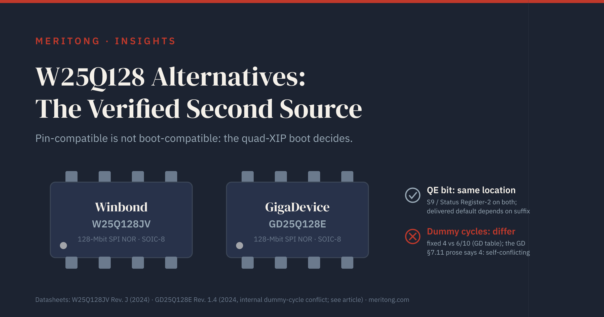
The Winbond W25Q128, a 128-Mbit (16-MB) SPI NOR flash, is a widely used and widely second-sourced part in embedded design, and an easy one to get wrong. The trap is specific: a "pin-compatible" alternative can pass every bench test that avoids the quad boot path and still fail to boot in production, because the failure sits in the execute-in-place (XIP) boot configuration, not in ordinary reads.
A verified SPI NOR cross-reference has to match more than density, voltage, and pinout. It has to match how the part is put into quad mode: the Quad-Enable (QE) bit and, an easy parameter to miss, the number of dummy cycles the fast quad read uses, because your boot stage assumes a specific configuration and timing. Using the W25Q128JV and a commonly considered alternative, GigaDevice's GD25Q128E, as the worked example, here's the surprising part: the QE bit sits at the same register location on both. But the delivered QE default doesn't necessarily match (on the Winbond it depends on the ordering suffix), and the dummy cycles don't match either. Each mismatch on its own can leave the current firmware unable to boot from the replacement flash.
Why a flash that boots on the bench can fail in the field
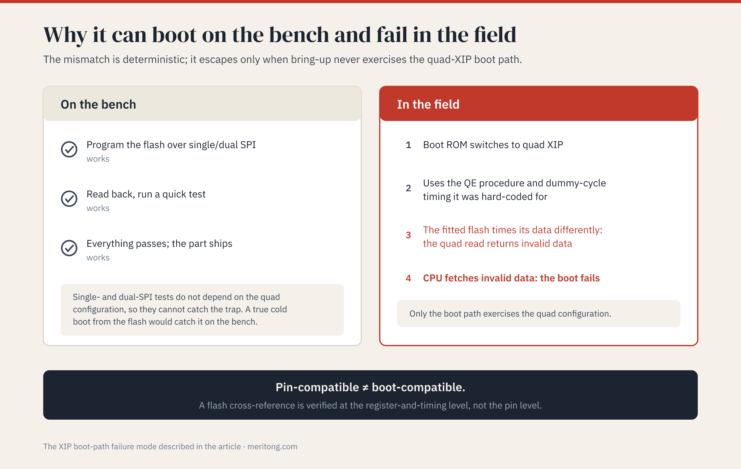
When a microcontroller runs code directly out of external flash (execute-in-place), it usually does so over Quad SPI (four data lines, IO0–IO3, plus clock and chip-select) for speed, and it configures the flash for that at boot: enable the quad data lines, then issue a fast quad read with a specific number of "dummy" clock cycles between the address phase and the returned data. If any of those steps assumes the wrong register, bit, or timing for the flash that's actually fitted, the quad read returns invalid data and the processor fetches nonsense instructions. Nothing is damaged, and the part isn't destroyed; the system simply fails to boot. That's the failure engineers loosely call "bricking" the boot, and recovering from it means reprogramming or reconfiguring, not replacing hardware.
One distinction matters before going further: boot ROM and bootloader are not the same stage. The boot ROM is normally immutable code inside the processor, and on many parts it performs the very first access to the external SPI NOR, typically to load a first-stage bootloader stored in that same flash. If the ROM can't read the replacement flash, your bootloader never gets the chance to run, and no later software can repair the ROM's assumptions. On other architectures, a bootloader running from internal flash or RAM configures the external flash before using it, and that code you can update. Where the difference doesn't matter, this article says "boot stage."
A QE or dummy-cycle mismatch is deterministic: it shows up every time the affected boot path actually runs. So how does a bad substitute get through a bench? Only when the bench never exercises that path. The typical escape routes: the programmer verifies its work over plain single-line (1-1-1) SPI reads, which don't depend on the quad configuration; the test procedure never performs a true cold boot from the external flash; the debug or development boot path differs from the production one; a development fixture has already configured the flash, and a QE or dummy-configuration bit set once by a bring-up script survives, because those bits are non-volatile; warm-reset state differs from power-on state; or the margin only collapses at production clock speed or at voltage and temperature corners. The fix for all of these is the same: test the real boot path, cold, on the real hardware. A flash cross-reference has to be verified at the register-and-timing level, not the pin level.
W25Q128 vs GD25Q128: what actually matches, and what doesn't
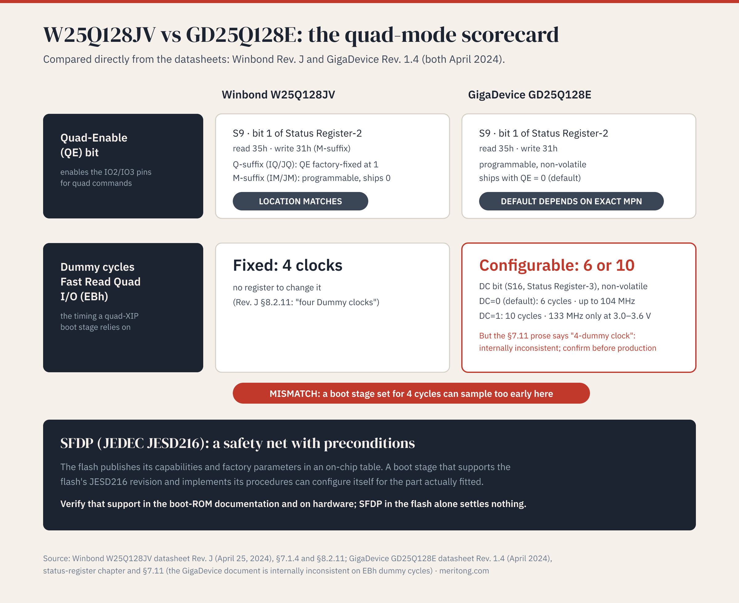
I read both current datasheets, Winbond's W25Q128JV (Rev. J, April 25, 2024) and GigaDevice's GD25Q128E (Rev. 1.4, April 2024), specifically to compare the quad-mode configuration. The result is a useful lesson in not assuming where the gotcha is:
The QE register location matches; the delivered QE state may not. Both families put the Quad-Enable bit at S9, bit 1 of Status Register-2, read with opcode 35h and, on the variants where it's programmable, written with 31h. That's where the folklore-level match ends, because Winbond ties the QE default to the ordering suffix. Per §7.1.4 of the Rev. J datasheet, QE=0 is the "factory default for part numbers with ordering options 'IM' & 'JM'" (a programmable, non-volatile bit), while QE=1 is the "factory fixed default for part numbers with ordering options 'IQ/IN' & 'JQ'". The GD25Q128E's QE bit is programmable, non-volatile, and defaults to 0 (Rev. 1.4, Table 7 and the QE-bit description). Replace a Q-suffix Winbond, whose QE is fixed at 1 with the quad pins always enabled, with a GigaDevice part that arrives at QE=0, and a boot stage that never sets QE (because it never had to) will fail its quad read. So the register location matches, but QE compatibility can only be judged against the complete orderable part number, not against "W25Q128" or even "W25Q128JV."
The dummy cycles don't match, and GigaDevice's own datasheet is internally inconsistent about them. For the Fast Read Quad I/O command (EBh), the W25Q128JV datasheet (Rev. J, §8.2.11) specifies four dummy clocks after the mode byte, with no register to change them. The GD25Q128E Rev. 1.4 DC-bit table (DC, the Dummy Configuration bit, S16 in Status Register-3) specifies six dummy cycles at the default DC=0 for operation up to 104 MHz, or ten at DC=1 for up to 133 MHz, and the 133 MHz rating carries an "R" footnote restricting VCC to 3.0–3.6 V. The EBh timing diagram appears consistent with the six-cycle default. But the prose in §7.11 of the same document says "4-dummy clock," apparently contradicting the table and the diagram. The table and diagram are the more credible reading; still, a production qualification should confirm the actual behavior with GigaDevice and on representative hardware rather than treat this datasheet as unambiguous. The practical risk stands either way: a host configured for Winbond's four cycles can begin sampling before a six-cycle-configured GD25Q128E has started returning valid data, and the quad boot fails even with QE set correctly.
That's the whole point of a verified cross-reference: for this pair, the trap is not where the folklore puts it (the QE register location). It's in the delivered defaults and the timing, and one of the two datasheets contradicts itself. You only find any of that out by reading the documents, and where they disagree, by asking the vendor and testing the silicon.
And EBh compatibility is more than QE plus a dummy count. Host and flash have to agree on the whole transaction: the opcode, the 1-4-4 command/address/data line widths, the three-byte address phase, the mode byte's value and its continuous-read ("XIP mode") entry and exit rules, any wrap configuration in use, and how the part gets back to a known protocol state after a reset. Any one of those, mismatched, produces the same symptom: a read that returns invalid data.
SFDP: a safety net with preconditions
SFDP (Serial Flash Discoverable Parameters) is the JEDEC standard (JESD216) by which a flash publishes its supported capabilities and factory parameters in a small on-chip table: fast-read opcodes, mode-clock and wait-state (dummy) counts and, in the applicable JESD216 revisions, a defined procedure for setting Quad Enable. Both parts here implement the mechanism (opcode 5Ah). A boot stage that reads SFDP can configure itself for the part actually fitted instead of assuming one.
Microchip's SAM9X60 documentation is a concrete example of one such implementation. Its boot ROM sends the flash a software reset, looks for SFDP tables (it supports JESD216, JESD216A, and JESD216B), applies the discovered op code and timing settings, and executes the Quad-Enable procedure indicated by bits [22:20] of DWORD15 in the Basic Flash Parameter table; only if no SFDP is found does it fall back to hard-coded per-manufacturer settings selected by JEDEC ID. That is how one specific boot ROM behaves. It is not evidence that yours behaves the same way.
So treat SFDP as conditional, not automatic. SFDP can reduce part-specific assumptions if the earliest boot stage supports the flash's JESD216 revision, parses the relevant fields, and implements the indicated read and Quad-Enable procedures. That stage is often immutable ROM: if it doesn't do these things for your flash, no later bootloader can repair it. Some boot ROMs parse only particular SFDP revisions or a limited subset of fields. SFDP also describes capabilities and factory defaults, not the current contents of writable non-volatile bits: it won't tell you that a QE or dummy-configuration bit has been changed since the part left the factory. And vendor-specific quirks or plain errors in a part's SFDP table exist. So the capability has to be verified twice: once in the processor's boot-ROM documentation, and once on the actual hardware.
Other W25Q128 alternatives: the same discipline applies
GigaDevice's GD25Q128E is a commonly considered W25Q128 alternative, but it isn't the only one: 128-Mbit SPI NOR is a crowded category, with pin-compatible candidates from XMC, Macronix, ISSI, Puya, and others. I'm deliberately not going to quote their register maps here, because I only opened the Winbond and GigaDevice datasheets for this piece, and the entire point of this article is that you verify each candidate against its own datasheet rather than trust a "128 Mbit SPI NOR, SOIC-8" label. The GD25Q128E lesson generalizes into a warning, not a shortcut: even a close alternative that matched on the QE register location still differed on delivered defaults and dummy cycles, and its datasheet needed a second, skeptical reading. A more distant alternative can differ on the QE register itself, the SFDP contents, the write-protection scheme, or the voltage class, any of which can be the thing that stops your boot.
There's also a voltage split to watch across the category: many of these parts come in both a ~2.7–3.6 V family and a separate 1.8 V family, sometimes distinguished only by a suffix. Voltage compatibility cuts both ways, and "won't work" understates it: a 1.8 V-class flash exposed to a 3.3 V supply can exceed its absolute maximum ratings and be permanently damaged, while a 3.3 V-class part supplied from a 1.8 V rail will generally not meet its operating conditions. Check the supply range and the I/O levels, and confirm the voltage class of every candidate before you look at anything else.
The practical stance: treat every 128-Mbit SPI NOR alternate as a candidate to screen with the checklist below against its own datasheet, then qualify the exact orderable part on your hardware. SFDP, where your boot stage genuinely supports it, narrows the risk; it doesn't remove the need to verify.
The SPI NOR cross-reference checklist: screening, then qualification
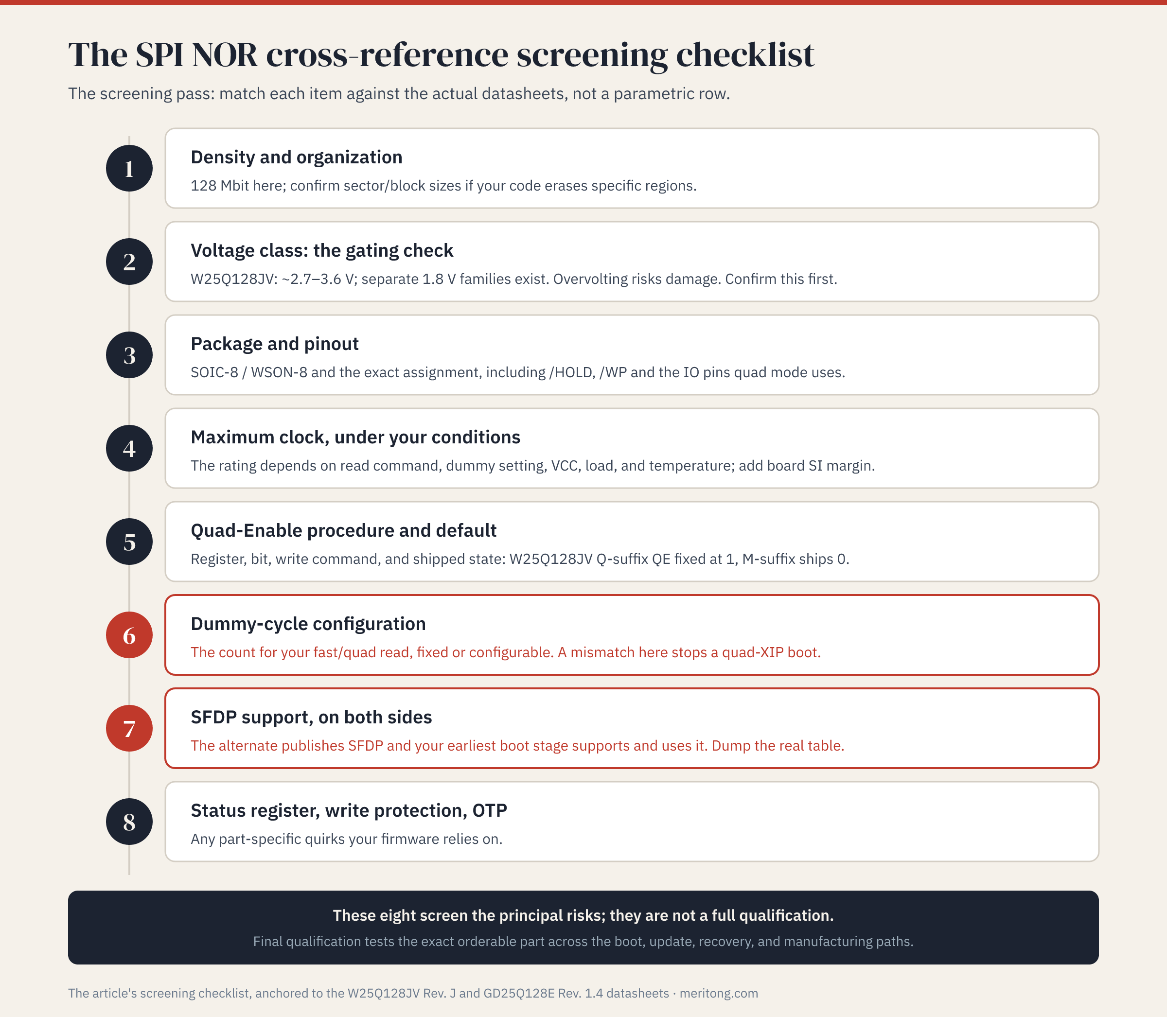
Screen candidates against the actual datasheets, not a parametric row:
Density and organization: 128 Mbit here, and confirm sector/block erase sizes and opcodes if your code erases specific regions.
Voltage: a gating check. The common W25Q128JV is a ~2.7–3.6 V part; there are separate 1.8 V-class families. Overvolting a 1.8 V part risks permanent damage; undervolting a 3.3 V part means it won't meet spec. Confirm the supply range and I/O levels first.
Package, pinout, and board wiring: SOIC-8 / WSON-8 dimensions, exposed pad and land pattern, the exact pin assignment, and how /WP and /HOLD (or /RESET) are wired on your board. Pull-ups versus hard ties matter once quad mode repurposes those pins as IO2/IO3.
Maximum clock, under your conditions: the rating depends on the specific read command, the dummy setting, VCC, output load, and temperature. The GD25Q128E's 133 MHz EBh rating, for example, requires the ten-cycle DC=1 setting and 3.0–3.6 V. Your real ceiling also involves controller sampling timing and board signal integrity.
Quad-Enable procedure and default: which register and bit, the write command, whether it's volatile or non-volatile, and the state the part ships in, which can hinge on the ordering suffix (W25Q128JV: Q-suffix QE fixed at 1, M-suffix programmable with default 0).
Dummy-cycle configuration: the count for your fast/quad read, whether it's fixed or configurable, and the non-volatile state it will actually be in on your boards. A mismatch here is what leaves the current firmware unable to boot from the replacement flash.
SFDP support, on both sides: the alternate publishes SFDP, and your earliest boot stage supports that SFDP revision and actually uses it. Dump and compare the real table contents; don't assume them.
Status-register layout, write protection, and OTP behavior: the write semantics of the 01h/31h-style status commands, block-protection and lock bits, security registers, and any part-specific quirks your firmware relies on.
Those eight screen for the failure modes this article is about. Screening, though, is not qualification. A full second-source qualification also compares, from the datasheets and on real hardware:
Part identity: the exact orderable part number (MPN), suffix, and silicon revision; the JEDEC manufacturer/type/capacity ID and any ID whitelist in your firmware or tools (the W25Q128JV's JEDEC device ID itself differs between suffixes: 4018h for IN/IQ/JQ versus 7018h for IM/JM); the SFDP revision, plus an actual dump of the SFDP contents.
Addressing: density and address width, 3-byte versus 4-byte addressing, bank or extended-address registers, and dedicated 4-byte opcodes where relevant.
Protocol state: every read protocol and opcode you use, with its command/address/mode/data line widths, mode- or alternate-byte requirements, continuous-read/XIP entry and exit, wrap configuration, software and hardware reset commands, and recovery from an unknown protocol or continuous-read state.
Program and erase: sector and block erase sizes and opcodes, page-program size and page-boundary wrap behavior, program/erase suspend and resume, and behavior after an interrupted program or erase.
Electrical and reliability: temperature range and qualification grade, power-on-reset thresholds, supply ramp rates and timing, standby/read/program/erase currents, endurance and retention against your requirements, and signal-integrity margin on the actual PCB.
The whole chain: compatibility with the complete boot, firmware-update, recovery, and manufacturing/programming toolchain, tested across cold boot, warm reset, brownout, and voltage and temperature corners.
These checks identify the principal compatibility risks. Final qualification still requires testing the exact orderable part in the intended boot, update, recovery, and manufacturing paths.
FAQ
What's the best low-difficulty term to know here: is "SPI NOR" the category?
Yes, SPI NOR flash is the category (serial NOR flash on the SPI/Quad-SPI bus, used for code storage and XIP boot). The W25Q128 is one specific 128-Mbit part in it, and the cross-reference method in this article applies across the category.
Is the GD25Q128 a drop-in for the W25Q128?
That can't be settled at the family level, and family level is what this article compares. Whether a specific GigaDevice part can replace a specific Winbond part depends on the complete orderable part numbers (the Winbond QE default differs between Q- and M-suffix parts), the delivered QE and dummy-configuration states, your boot stage's behavior (hard-coded timing or SFDP-driven), and a system-level qualification on your hardware. The register locations lining up at S9/SR-2 is necessary, but nowhere near sufficient.
What is the "QE bit" and why does it matter?
The Quad-Enable bit enables the IO2 and IO3 pins for quad commands: with QE set, Quad Output and Quad I/O reads can use all four data lines. Standard single-line (1-1-1) commands generally remain available; QE does not switch the whole device into a different protocol. (QPI or 4-4-4 operation, where a part supports it, is a separate protocol state entered by its own command, and shouldn't be conflated with setting QE.) It matters because quad boot requires it set correctly, and its location, procedure, and delivered default vary by manufacturer, by model, and even by ordering suffix.
What is SFDP and why do I want it?
SFDP is a JEDEC standard (JESD216) by which the flash publishes its supported parameters and factory defaults on-chip. A boot stage that supports the flash's SFDP revision and implements its procedures can configure itself for whatever flash is present, which makes cross-referencing meaningfully safer. It is not automatic, though: the boot ROM has to actually parse those tables and act on them (some parse only particular revisions or fields), SFDP can't report the current state of writable non-volatile bits, and SFDP tables have shipped with errors. Verify support in the processor's boot documentation and on hardware.
Why did my board boot on the bench but not in production after a flash change?
A quad-XIP configuration mismatch (QE default, dummy cycles) is one likely cause, since bench bring-up often runs over single/dual SPI and never exercises the quad boot path. But treat it as one hypothesis among several. Also check: a JEDEC-ID whitelist in the boot chain or programming tools, a continuous-read or QPI state left behind by an earlier stage, reset-behavior differences, power sequencing and power-on-reset thresholds, protection bits, signal integrity and clock margin at the production frequency, temperature or voltage corners, and erase/program behavior your updater assumes.
Do I need to worry about this if I don't use XIP?
Less, but not zero. If you copy code from flash into RAM at boot rather than executing in place, a quad-timing mismatch is less likely to stop the boot, but you still lean on quad or dual reads for speed, and QE-bit and dummy-cycle differences can corrupt those reads too. The safe habit is the same: verify the configuration of the earliest read path against the exact part.
Is a higher-density flash (e.g. 256 Mbit) a safe replacement for a 128 Mbit?
Treat it as a redesign-level change, not a substitution. 128 Mbit is 16 MiB: exactly the ceiling of a 24-bit, 3-byte address. A 256-Mbit part needs a 25th address bit, which typically means 4-byte address mode, dedicated 4-byte opcodes, or an extended-/bank-address register, and your boot ROM, firmware, update tooling, and recovery path all have to support whichever of those the part uses. A boot stage that speaks only 3-byte addressing may or may not cope with the larger part, even within the first 16 MiB: that's a qualification question, not an assumption. Matching package and voltage does not make higher density safe.
Are Chinese SPI NOR flash parts (GigaDevice, XMC, Puya) safe second sources?
They're widely used parts. "Safe" is a function of verification, not origin: any alternate, from any vendor, has to be checked against its own datasheet for QE behavior, dummy cycles, SFDP, and voltage class, and then qualified as an exact part number on your hardware. The origin isn't the risk; skipping the verification is.
What's the single most important check on a flash cross-reference?
Verify the complete earliest boot transaction, with the exact orderable part fitted, on your hardware: a true cold boot, from power-on, through whatever read command and configuration your boot stage actually issues. Then confirm the update and recovery paths. SFDP support in both the flash and the boot stage reduces risk substantially, but it's the transaction test that settles the question.
Conclusion
A SPI NOR flash cross-reference based on pins and density is a latent boot failure waiting for production. Based on QE behavior, dummy cycles, SFDP, and the exact orderable part number, it's a second source you can plan around. These register-and-timing checks are the screening pass, not the whole job: real qualification still tests the boot, programming, firmware-update, and recovery chain with the actual part on representative hardware. A Second-Source Map does the screening the way it needs to be done — register by register, timing by timing, against both current datasheets and your boot path — and names exactly what still needs to be qualified on hardware. That's what makes the alternative that boots on the bench also boot in production. For a part as widely second-sourced as the W25Q128, that discipline is the difference between a qualified alternate and a field-return wave. If it helps: that's exactly what we do.
This article cites specific datasheet revisions: Winbond W25Q128JV Rev. J (April 25, 2024), the standard SPI variant datasheet (the DTR variant has a separate document, W25Q128JV-M DTR); GigaDevice GD25Q128E Rev. 1.4 (April 2024, document DS-00480), whose prose in §7.11 contradicts the DC-bit table as noted above; and Microchip's SAM9X60 datasheet, section "QSPI NOR Flash Boot." Other parts and revisions will differ. This is general engineering guidance, not a specification for any particular part. Verify the exact part and revision against its datasheet and your boot stage before committing.
Get the next pattern by email
One dependency pattern from real hardware audits, occasionally. No schedule promised yet.
Working through this right now? Book a call → or write to me →